Graphene was very first discovered experimentally in 2004, bringing hope to the growth of high-performance electronic tools. Graphene is a two-dimensional crystal made up of a solitary layer of carbon atoms set up in a honeycomb form. It has an one-of-a-kind electronic band structure and outstanding digital properties. The electrons in graphene are massless Dirac fermions, which can shuttle bus at exceptionally fast rates. The carrier mobility of graphene can be more than 100 times that of silicon. “Carbon-based nanoelectronics” based upon graphene is anticipated to usher in a new era of human details culture.

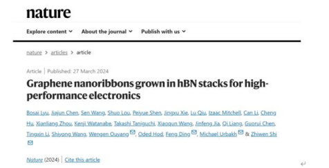
(Graphene nanoribbons grown in hBN stacks for high-performance electronics on “Nature”)
Nonetheless, two-dimensional graphene has no band void and can not be straight made use of to make transistor devices.
Academic physicists have suggested that band voids can be introduced through quantum arrest effects by cutting two-dimensional graphene into quasi-one-dimensional nanostrips. The band void of graphene nanoribbons is inversely symmetrical to its width. Graphene nanoribbons with a width of less than 5 nanometers have a band space similar to silicon and are suitable for producing transistors. This kind of graphene nanoribbon with both band space and ultra-high wheelchair is one of the optimal candidates for carbon-based nanoelectronics.
Therefore, scientific researchers have actually spent a great deal of power in examining the prep work of graphene nanoribbons. Although a variety of techniques for preparing graphene nanoribbons have actually been created, the trouble of preparing premium graphene nanoribbons that can be utilized in semiconductor gadgets has yet to be solved. The carrier flexibility of the ready graphene nanoribbons is much lower than the theoretical values. On the one hand, this difference originates from the poor quality of the graphene nanoribbons themselves; on the various other hand, it comes from the disorder of the atmosphere around the nanoribbons. Due to the low-dimensional buildings of the graphene nanoribbons, all its electrons are subjected to the external atmosphere. Therefore, the electron’s motion is exceptionally easily impacted by the surrounding setting.
(Concept diagram of carbon-based chip based on encapsulated graphene nanoribbons)
In order to enhance the efficiency of graphene devices, several methods have actually been attempted to reduce the condition effects triggered by the setting. One of the most effective approach to date is the hexagonal boron nitride (hBN, hereafter referred to as boron nitride) encapsulation approach. Boron nitride is a wide-bandgap two-dimensional layered insulator with a honeycomb-like hexagonal lattice-like graphene. Extra significantly, boron nitride has an atomically flat surface area and excellent chemical security. If graphene is sandwiched (encapsulated) in between two layers of boron nitride crystals to develop a sandwich structure, the graphene “sandwich” will certainly be isolated from “water, oxygen, and bacteria” in the complex exterior atmosphere, making the “sandwich” Constantly in the “best quality and best” problem. Multiple research studies have shown that after graphene is encapsulated with boron nitride, several residential or commercial properties, consisting of carrier wheelchair, will certainly be substantially enhanced. Nevertheless, the existing mechanical packaging methods might be extra efficient. They can currently only be utilized in the field of scientific research, making it tough to satisfy the needs of large-scale production in the future innovative microelectronics market.
In feedback to the above difficulties, the team of Professor Shi Zhiwen of Shanghai Jiao Tong University took a new method. It created a brand-new prep work approach to achieve the embedded development of graphene nanoribbons between boron nitride layers, developing an unique “in-situ encapsulation” semiconductor residential or commercial property. Graphene nanoribbons.
The development of interlayer graphene nanoribbons is attained by nanoparticle-catalyzed chemical vapor deposition (CVD). “In 2022, we reported ultra-long graphene nanoribbons with nanoribbon lengths up to 10 microns expanded externally of boron nitride, but the length of interlayer nanoribbons has far exceeded this record. Now limiting graphene nanoribbons The ceiling of the length is no longer the development system but the dimension of the boron nitride crystal.” Dr. Lu Bosai, the first writer of the paper, said that the length of graphene nanoribbons expanded in between layers can reach the sub-millimeter level, far surpassing what has actually been formerly reported. Result.
(Graphene)
“This type of interlayer ingrained growth is outstanding.” Shi Zhiwen claimed that product growth typically includes growing another on the surface of one base material, while the nanoribbons prepared by his research team grow straight on the surface of hexagonal nitride between boron atoms.
The aforementioned joint study group worked closely to reveal the growth system and discovered that the formation of ultra-long zigzag nanoribbons in between layers is the result of the super-lubricating properties (near-zero friction loss) between boron nitride layers.
Speculative monitorings show that the development of graphene nanoribbons only occurs at the particles of the stimulant, and the placement of the stimulant remains the same throughout the procedure. This shows that the end of the nanoribbon exerts a pushing force on the graphene nanoribbon, triggering the entire nanoribbon to overcome the friction between it and the bordering boron nitride and continually slide, triggering the head end to relocate away from the stimulant particles progressively. For that reason, the scientists speculate that the friction the graphene nanoribbons experience have to be extremely tiny as they move between layers of boron nitride atoms.
Considering that the grown up graphene nanoribbons are “enveloped in situ” by protecting boron nitride and are protected from adsorption, oxidation, ecological contamination, and photoresist call during gadget processing, ultra-high efficiency nanoribbon electronics can theoretically be gotten gadget. The researchers prepared field-effect transistor (FET) devices based upon interlayer-grown nanoribbons. The measurement results showed that graphene nanoribbon FETs all displayed the electrical transportation attributes of common semiconductor gadgets. What is more noteworthy is that the gadget has a carrier mobility of 4,600 cm2V– 1s– 1, which exceeds previously reported results.
These exceptional residential properties indicate that interlayer graphene nanoribbons are expected to play an essential function in future high-performance carbon-based nanoelectronic devices. The study takes a vital step toward the atomic construction of innovative packaging architectures in microelectronics and is expected to influence the field of carbon-based nanoelectronics dramatically.
Provider
Graphite-crop corporate HQ, founded on October 17, 2008, is a high-tech enterprise committed to the research and development, production, processing, sales and technical services of lithium ion battery anode materials. After more than 10 years of development, the company has gradually developed into a diversified product structure with natural graphite, artificial graphite, composite graphite, intermediate phase and other negative materials (silicon carbon materials, etc.). The products are widely used in high-end lithium ion digital, power and energy storage batteries.If you are looking for graphene nanotechnology, click on the needed products and send us an inquiry: sales@graphite-corp.com
Inquiry us